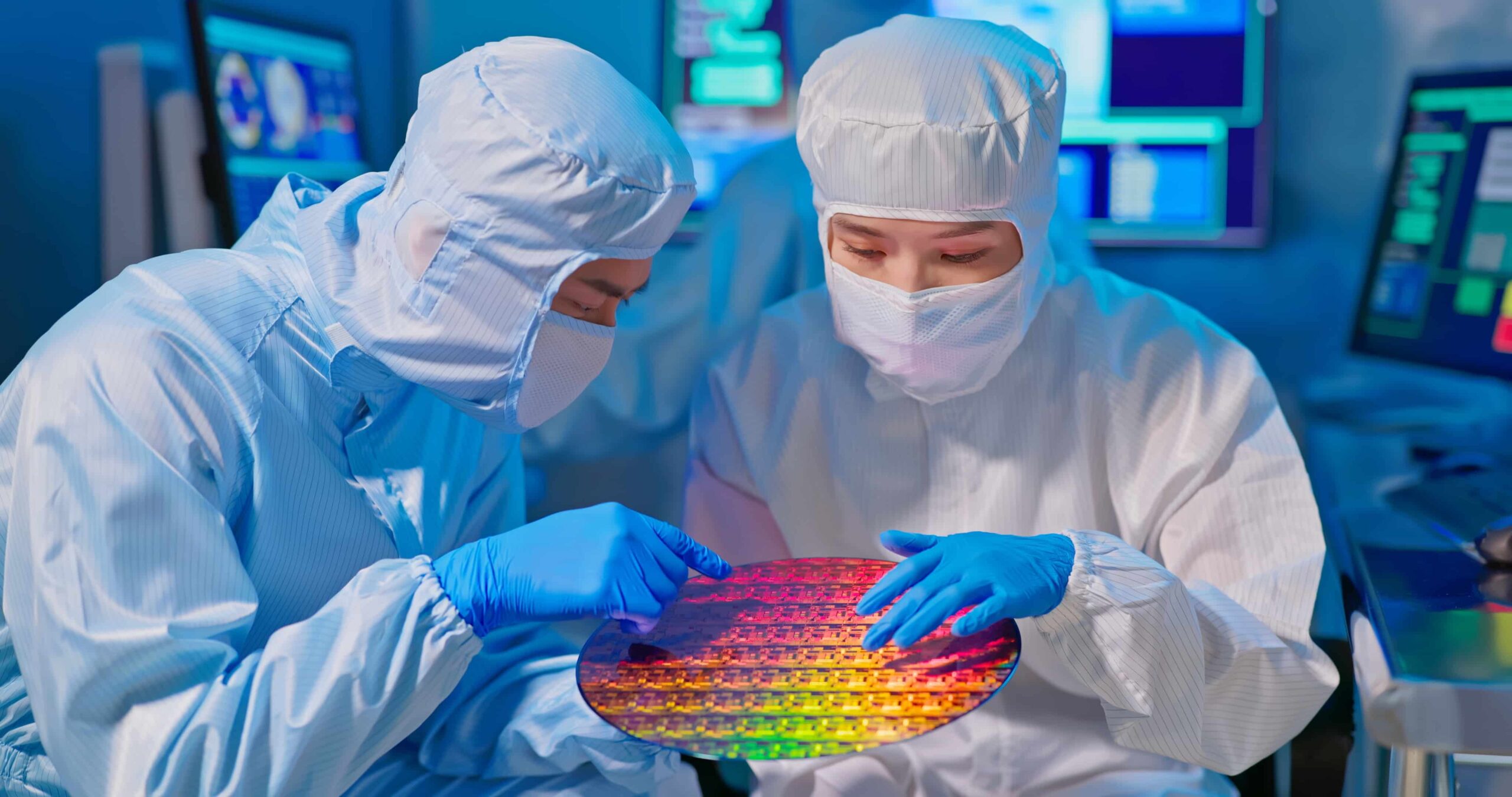

Wafer Fab II
Here’s where next gen wafers multiply and keep your world moving
Global demand for chips that power our society – from smart phones to laptops, electric cars and aircrafts – is increasing significantly. One of the world’s six largest silicon wafer manufacturers, plans to realise a new, state-of-the art 300mm EPI wafer production facility. Before project take-off Deerns conducted a feasibility study for the new production line, including a budget estimate while translating every detail of the requirements into a state-of-the-art building with optimised logistics. Indeed this integrated outline ensures that project execution enables time-to-market requirements, thereby eliminating the current shortage of chips for electronic devices.
