Location
Milan, Italy
Size
6 000 m² + cleanroom
Client
Global Wafers
Completion
2024
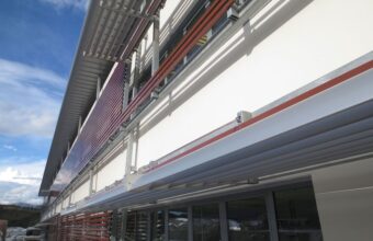
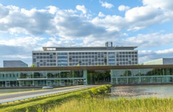
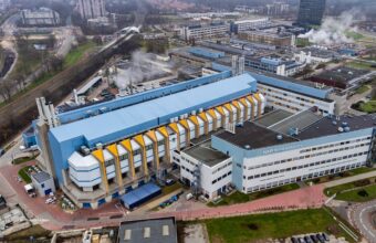
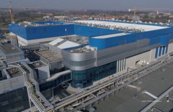
Deerns engineered a cutting-edge production facility in Italy for one of the world’s largest silicon wafer manufacturers, Global Wafers.
Location
Milan, Italy
Size
6 000 m² + cleanroom
Client
Global Wafers
Completion
2024
Strategic Expansion for Next-Generation Silicon Wafer Production
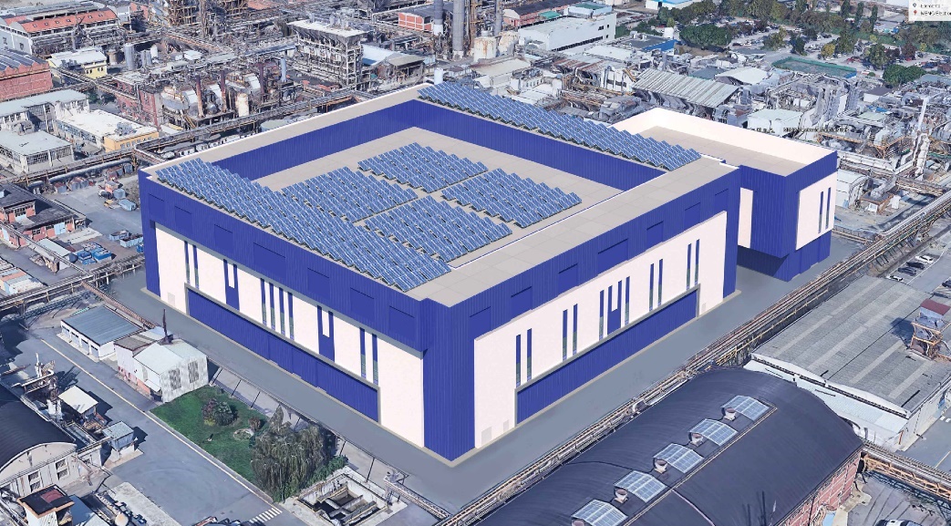
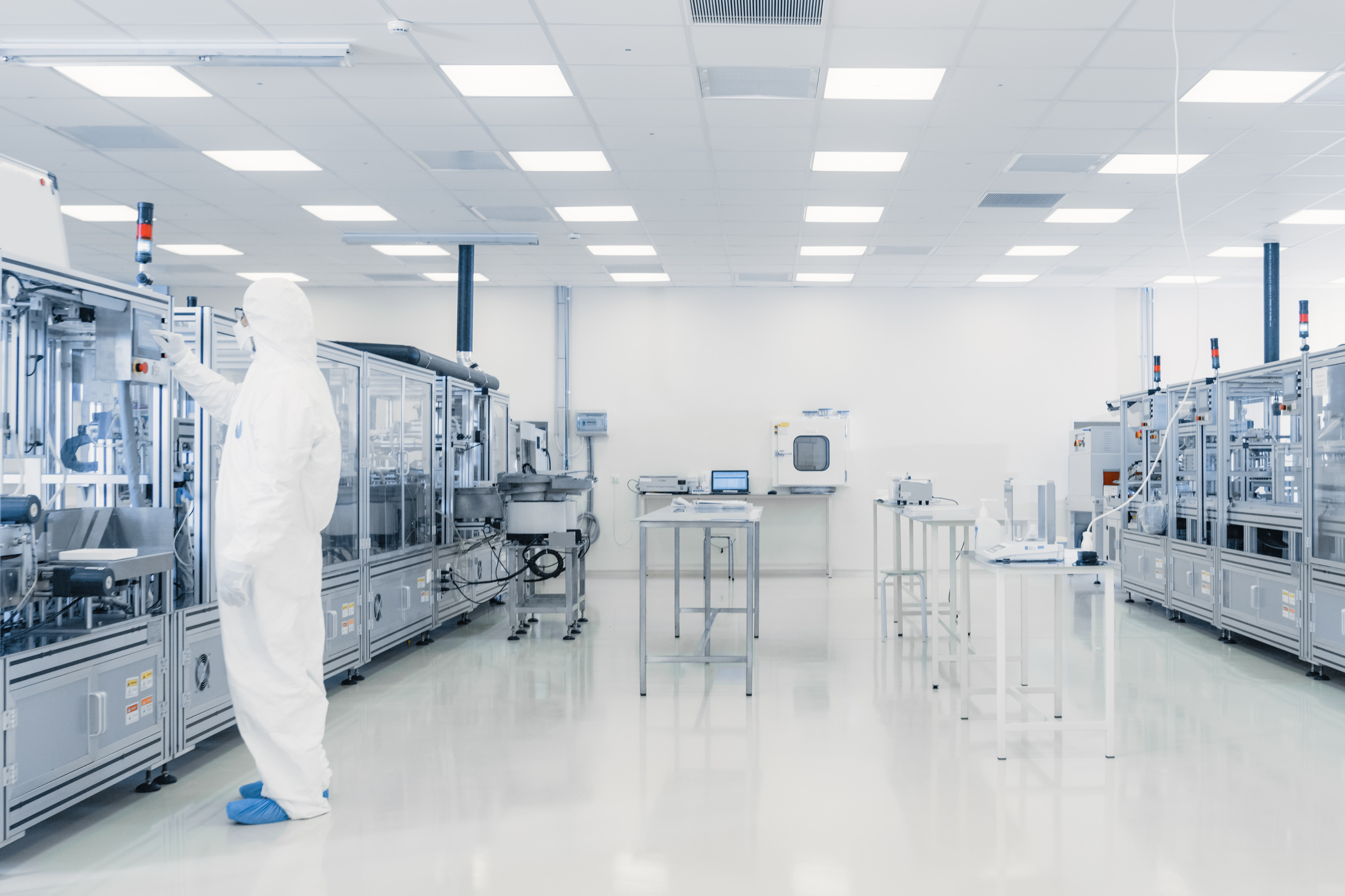
Global Wafers undertook a new, state-of-the art production facility in Italy to meet demand for new-generation high-purity 300mm EPI wafers. The project encompassed expanding an existing factory and creating a new one. Deerns conducted an all-round feasibility study for this new production line.
Through this extensive study, Deerns investigated the options for this site expansion including a budget cost estimate. Using the detailed client requirements, we were able to advise on feasible solutions for a state-of-the-art building with optimised planning. Our feasibility study enabled careful, fact-based decision-making by Global Wafers. As a result, a different site was selected for quicker turnaround time of the entire project.
The layout of the facility includes a sub-fab at ground level; the 6,000m2 cleanroom at first floor level; a plenum on the third floor and two laterals on the sides of the building for distribution. A central utility building of three storeys will house the main plant rooms.
Deerns was involved in construction management of critical process systems: high purity gases and chemicals supply, and ultrapure water systems; reviewing design for construction; supervising execution of the works; commissioning, qualification and validation of these systems.
Scope of Deerns
- Feasibility study
- Construction management
- Process Critical Systems Engineering (PCS)
- Design review
- Clerk of works
- Commissioning, qualification and validation
Scope of Deerns
Construction Management, Supervision & Commissioning
A well-crafted building design must be expertly executed to achieve the desired outcome.
MEP
Deerns designs mechanical and electrical installations for buildings that are healthy, sustainable and safe.
Transactional Services
Buying or selling commercial real estate can be risky.

