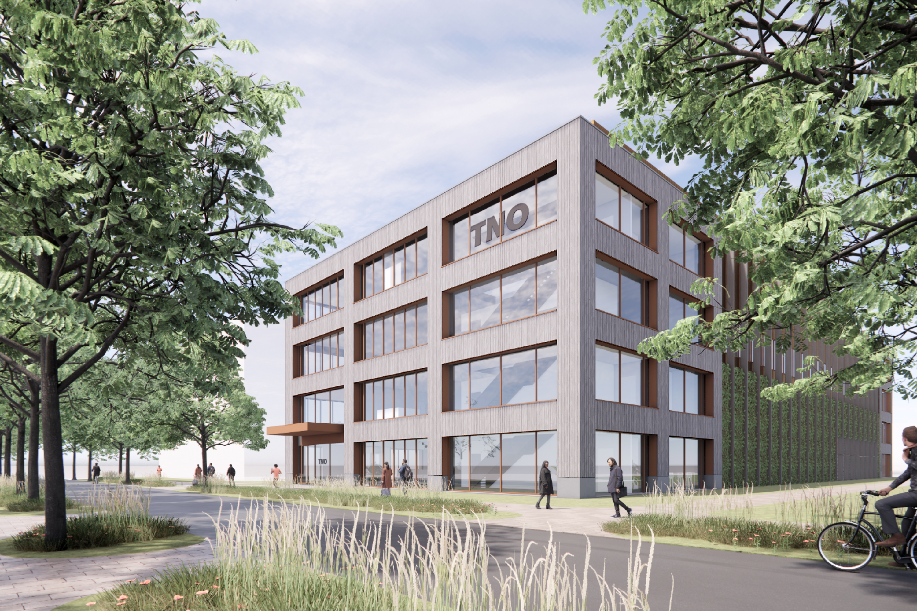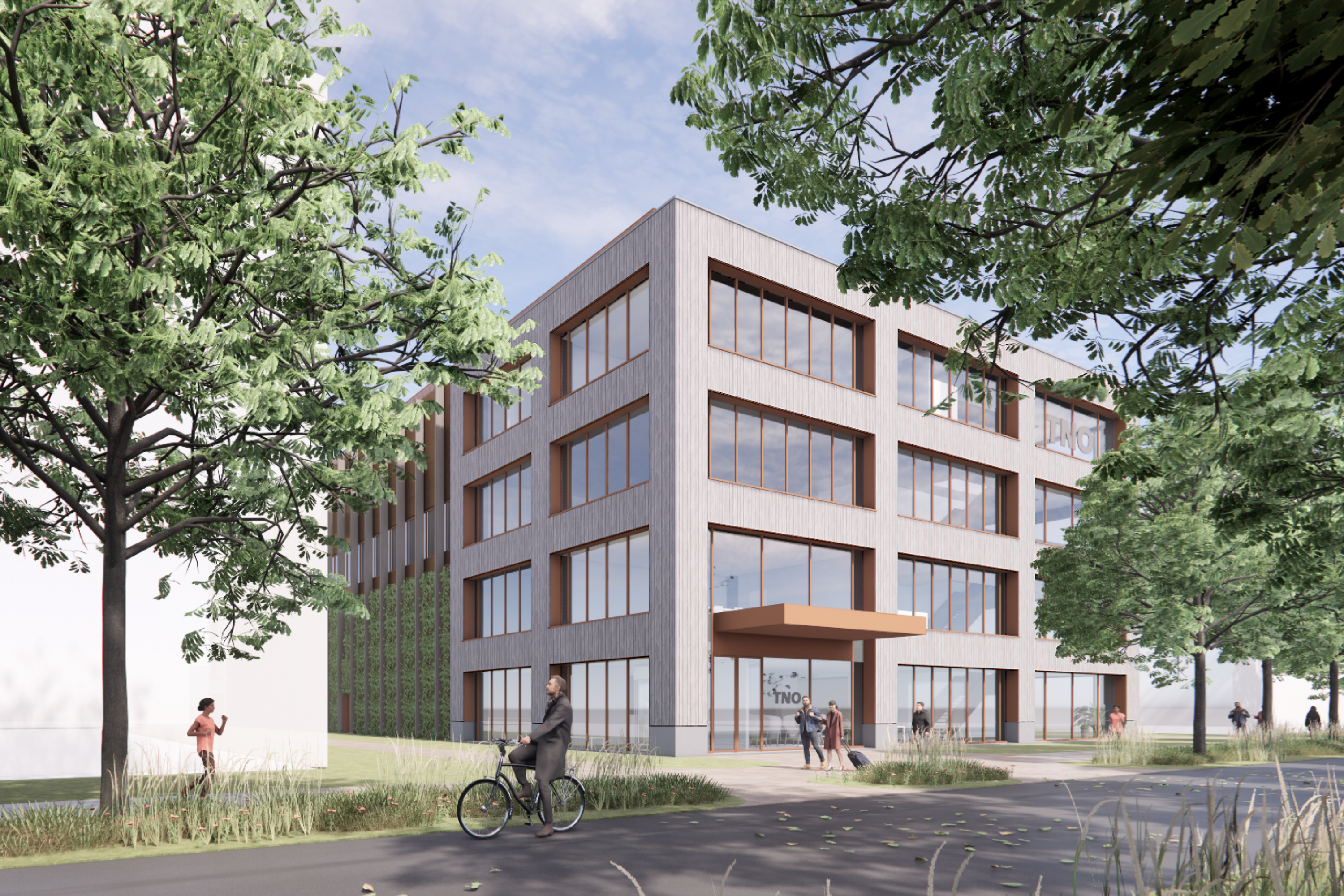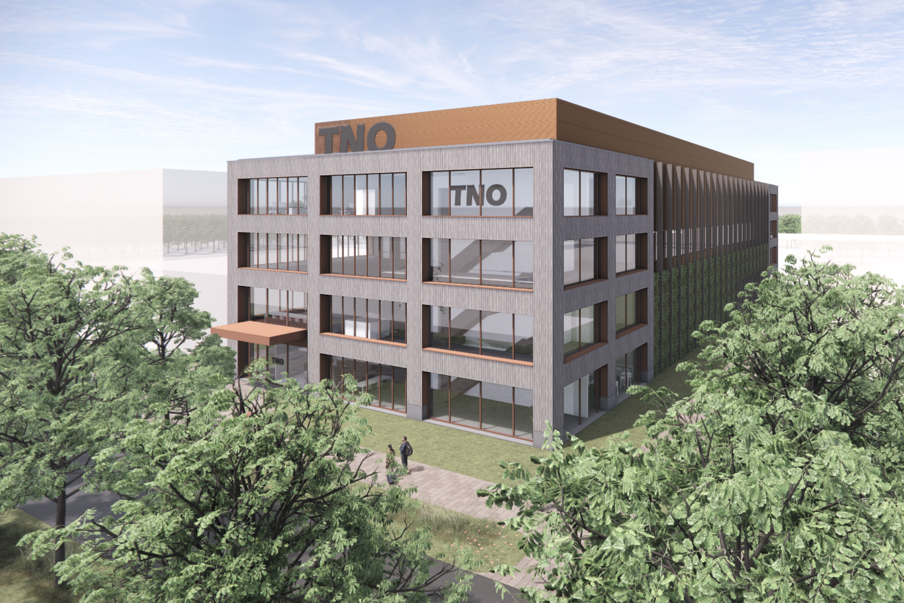
The Hague, 19 June 2025. Deerns is leading the high-precision clean room design for a pilot of new advanced photonic integrated circuits (PICs) at the High Tech Campus Eindhoven (HTCE), as part of PIXEurope.
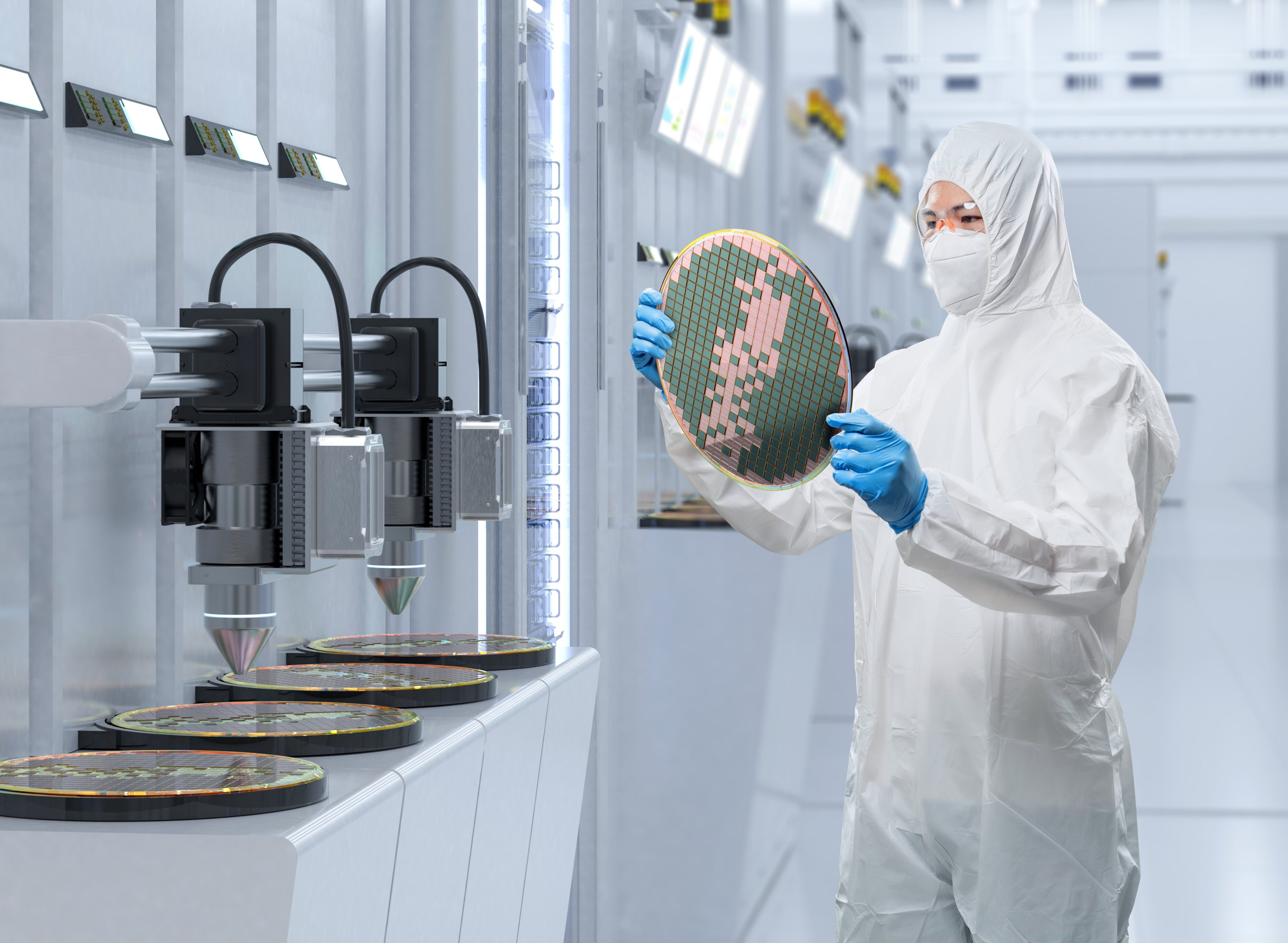
Within the framework of the European Chips Act, the European Commission announced the creation of PIXEurope, a new European pilot line for photonic chips. The initiative aims to accelerate the development and industrialisation of PICs, positioning Europe as a global leader in photonics. It will enable the transformation and transfer of disruptive integrated photonics processes and technologies, driving their rapid industrial adoption.
Strategic Deep Tech Investment
The pilot line at HTCE is a strategic investment in Europe’s technological future and is backed by €153 million in funding from the EU Chips Act, PhotonDelta, TNO, and Dutch ministries. HTCE will invest in the building and high-quality cleanrooms dedicated to the development and pilot production of photonic devices. Deerns is responsible for the technical design of the new cleanroom facility together with Broekbakema Architects and Tielemans Building
Jeroen Triepels, Director of Operations, HTCE says of the cleanroom design for this game-changing pilot: “Through this major European collaboration between knowledge institutions, governmental institutions and private companies, we’re boosting Europe’s photonics ecosystem by facilitating cutting-edge engineering and deep-tech expertise. With this facility, we’re laying the foundation for breakthroughs in photonic technology that will deliver transformative improvements in speed and power-efficiency, precision powering future generations of data centres, smart devices, AI and advanced communications.”
Eric Stuiver, Sector Director Electronics, Deerns says, “I am proud to again be part of a crucial project for both HTCE and Europe,having taken my first steps at the HTCE in submicron semiconductors in 1986. Cleanrooms are the heart of advanced manufacturing. Together with HTCE and the other design partners we will ensure these spaces meet the highest standards of precision and quality.”
Three Distinct Photonic Features
Indium phosphide based photonics is used as a basis for optical transmission, which has promising features such as:
- low power consumption
- extensive transmission distance
- lower costs.
At a time when AI applications are booming, finding ways to cut energy consumption is a critical priority.
Every year, the needs of our digital society increase significantly – reflected in the projected global production of photonic integrated circuits (PICs), which is expected to increase by more than 400% over the next decade.
Deerns continues pacesetting in Semicon Industry
This project is reinforces the key role that Deerns has played in Brainport Eindhoven for over three decades. Since the mid-nineties, Deerns has been involved in the design for various laboratories, cleanrooms and energy projects on what was then the Philips Research Campus (NatLab). That role was extended when Philips sold the site in 2012 to a group of investors. Based on the unique knowledge and experience gained over this time, together with its local team in Eindhoven, Deerns has been one of the permanent design partners for various semicon companies for over 25 years.


